Samsung kicks off mass production of 3nm GAA chips: next-gen begins
Samsung beats TSMC to the 3nm mass production bunch: 3nm GAA chips in mass production, improvements in performance, power, more.
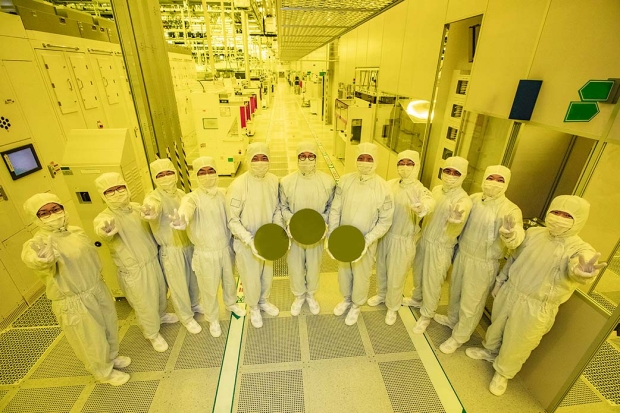
Samsung has announced that it has kicked off the initial production of its next-gen 3nm process node, using Gate-All-Around (GAA) transistor architecture.

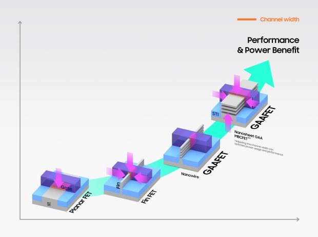
This is the first time Samsung's new Multi-Bridge-Channel FET (MBCFET), their new GAA technology, "defies the performance limitations of FinFET". It defies those performance limitations of FinFET by improving power efficiency by reducing the supply voltage level, while boosting performance through increasing drive current capability.
- Read more: Samsung wants to beat TSMC in 3nm manufacturing, 2nm coming in 2025
- Read more: Samsung is the first with a prototype 3nm design using GAAFET tech
Dr. Siyoung Choi, President and Head of Foundry Business at Samsung Electronics explains: "Samsung has grown rapidly as we continue to demonstrate leadership in applying next-generation technologies to manufacturing, such as foundry industry's first High-K Metal Gate, FinFET, as well as EUV. We seek to continue this leadership with the world's first 3nm process with the MBCFET™. We will continue active innovation in competitive technology development and build processes that help expedite achieving maturity of technology".

Samsung's new proprietary technology uses nanosheets with wider channels, which allows for more performance, and greater power efficiency compared to GAA technologies using nanowires with narrower channels. Samsung's use of 3nm GAA technology allows the company to tweak the channel width of the nanosheet in order to optimize power usage and performance for their various needs of their customer.
- Read more: TSMC announces FinFlex tech for N3 node, nanosheet-based N2 in 2025
- Read more: TSMC's next-gen 3nm yields are so good, production is starting earlier
- Read more: TSMC talks more about 3nm, hitting nails into Intel's Big Blue coffin
- Read more: TSMC to spend tens of billions more on US-based 3nm chip factories
- Read more: TSMC will make Intel CPUs on 3nm in 2022, largest order of 3nm process
- Read more: TSMC is so ahead of the game, Samsung might not catch up until 2030
The design flexibility of GAA is also a great thing for Design Technology Co-Optimization (DTCO), which helps boost Power, Performance, Area (PPA) benefits.

Samsung says that its first-generation 3nm process compared to its first-gen 5nm process reduces power consumption by up to 45%, boosts performance by up to 23%, and reduces area by 16%. Samsung goes one further, teasing that its second-gen 3nm process reduces power consumption by up to 50%, improvements in performance go up by 30%, and reduced area of 35%.
Samsung kicked off by prototyping a 3nm process using GAAFET (Gate-All-Around) technology back in January 2020. Regular Planar FET is 1 Gate on channel, FinFET is 3 Gates on channel, but the newer Gate-All-Around has 4 Gates on channel.


